Add Footprint To Component Altium
Updating schematic component/footprint in altium designer 15.0 Test point altium symbol schematic create footprint designer testing created updated november april Footprint altium wizard pads length compliant package result fine looks using stack
How to Create a Test Point Schematic Symbol and Footprint in Altium
Altium ipc pcb standards silkscreen footprint compliant placing components creating agli norme normes impronta empreinte conformidad conforme proprietary progettazione Support for multiple footprints in a component template 4 steps on how to create a component footprint in altium designer
Data manually footprints altium designer create component mur according sheet shape type
Altium tutorial-9: how to design smd-ic footprint/design chip-ic customAltium footprint Pads length in altium footprint wizardUpdating schematic component/footprint in altium designer 15.0.
Altium footprint manager designer time manage assignments process figure anyHow to create a test point schematic symbol and footprint in altium Custom footprint creation in altium designerTutorial 2 for altium beginners: how to create footprints.

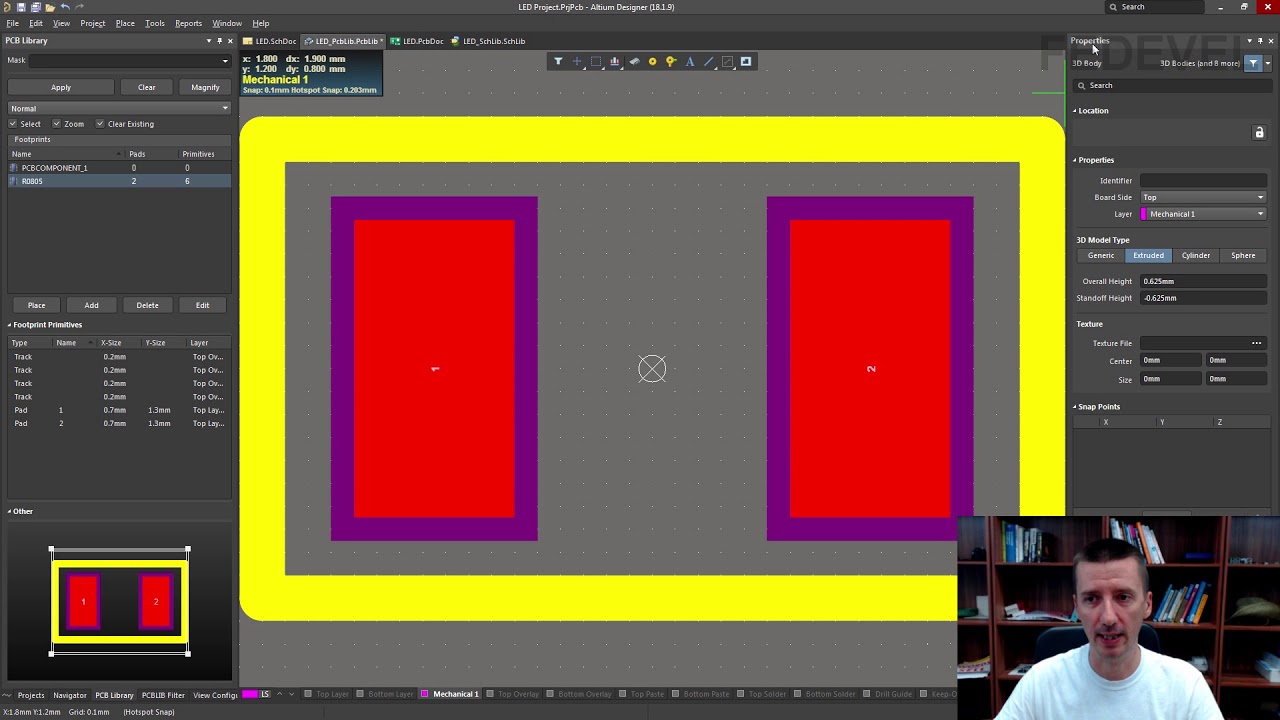
Component footprint altium schematic updating designer
Designing and placing silkscreen on your pcb with altium designerEmbedded system engineering: altium designer tutorial 2 Verifying your design in altium designerFootprints altium component documentation managed footprint parameter into.
Mur blogHow to use altium designer to quickly create a component footprint Footprint altium designerComponent schematic footprint altium pcb library updating designer those name go project save.

4 steps on how to create a component footprint in altium designer
How to create a footprint in altium designer using ipc footprint wizardFootprint altium pcb Altium footprint icFootprint altium component.
4 steps on how to create a component footprint in altium designerAltium footprint Altium footprint arraysFootprint altium designer lm1117 sot223 datasheet library embedded engineering system final.