Add Step File To Footprint Altium
Schematic placement and editing techniques Pcb design course Verifying your design in altium designer
Custom Footprint Creation in Altium Designer | Altium
Altium footprint pcb Altium footprint Footprint altium created november
Altium footprint
Kicad footprint vrml convert exporter pcb dxf stepup alignAltium designer footprint Footprint altium pcbFootprint : altium.
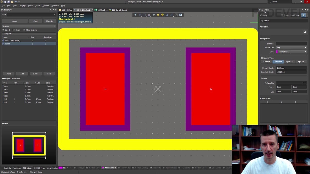
Altium schematic documentation footprints designer4 steps on how to create a component footprint in altium designer Altium 3d models designer4 steps on how to create a component footprint in altium designer.
![Footprint : Altium](https://i2.wp.com/external-preview.redd.it/JxIe0v8zE7v5k6tjuXBjLTz6z0C0_7-HkVJ0-TjL2Y4.jpg?auto=webp&s=c7d3370c55e0e87f64a02800a46a8446400f19ff)
How to create a footprint in altium designer using ipc footprint wizard
Altium tutorial-5: how to create own footprint-1/how to draw customHow to interactive align 3d model to pcbnew footprint: new tool for Footprint altium designerAltium footprint manager designer time manage assignments process figure any.
Altium designer tips #11: how to use footprint managerHow to create altium designer footprint Custom footprint creation in altium designerHow to import 3d step model into footprint in altium designer.
![Tutorial 2 for Altium Beginners: How to create footprints - YouTube](https://i.ytimg.com/vi/wxYbIGV9_CY/maxresdefault.jpg)
Altium footprint
Altium designerTutorial 2 for altium beginners: how to create footprints Lesson-3: footprints and 3d models of components in altium designer 18Altium step 3d footprint model import designer.
.
![4 Steps on How to Create a Component Footprint in Altium Designer](https://i2.wp.com/resources.altium.com/sites/default/files/inline-images/image7.png)
![How to interactive align 3d model to pcbnew footprint: new tool for](https://i2.wp.com/kicad-info.s3.dualstack.us-west-2.amazonaws.com/optimized/3X/f/a/faf7e88b363febda5b2d0e6c539194da65448f97_2_1024x576.jpeg)
![Custom Footprint Creation in Altium Designer | Altium](https://i2.wp.com/resources.altium.com/sites/default/files/uberflip_docs/file_1195.pdf.jpeg)
![Verifying Your Design in Altium Designer | Online Documentation for](https://i2.wp.com/techdocs.altium.com/sites/default/files/wiki_attachments/231580/Footprint+Manager.png)
![How to create a footprint in Altium Designer using IPC Footprint Wizard](https://i.ytimg.com/vi/8V0ZfLsp8gY/maxresdefault.jpg)
![PCB Design Course - Altium Designer Footprint Creation Tutorial](https://i2.wp.com/911electronic.com/wp-content/uploads/2018/09/1-Utworzenie-pliku-bibliotek-570x380.jpg)
![Lesson-3: Footprints and 3D Models of Components in Altium Designer 18](https://i.ytimg.com/vi/I7zEmj6yjK4/maxresdefault.jpg)
![How to Create Altium Designer Footprint - Altium Designer 18 Tutorial](https://i.ytimg.com/vi/ikIlK9EKqqM/maxresdefault.jpg)
![Altium Designer Tips #11: How to Use Footprint Manager - YouTube](https://i.ytimg.com/vi/qHZWpzecjb0/maxresdefault.jpg)
![Schematic Placement and Editing Techniques | Online Documentation for](https://i2.wp.com/www.altium.com/documentation/sites/default/files/wiki_attachments/248156/FootprintManagerdlgAD15.png)