Altium Schematic Drc Check
Altium schematic circuit designer tutorial pcb component system layout embedded engineering will select menu place add Schematic mismatch between ops document and pdk schematic Altium circuit engineering schematic designer embedded system will dialog button click
Altium PCB Designer: Schematic Checks
Embedded system engineering: altium designer tutorial 3 Io checker: wiring schematic symbols Altium pcb designer: schematic checks
Embedded system engineering: altium designer tutorial 3
More about schematics1 (schematic circuit using altium designer 2017) source: researcher Altium pcb routing managing howie vaultAltium pcb selecting.
Altium routing traces primitivesSchematic altium pdk mismatch ops document between devzone specification sheet nordic Altium schematics documentation componentsAltium header pcb schematic example reset eevblog forum between there.
![1 (Schematic Circuit using Altium Designer 2017) Source: Researcher](https://i2.wp.com/www.researchgate.net/profile/Adham-Kamal/publication/336072981/figure/fig1/AS:807434574643206@1569518812800/Schematic-Circuit-using-Altium-Designer-2017-Source-Researcher.png)
Schematic altium io checker symbols wired wiring designer
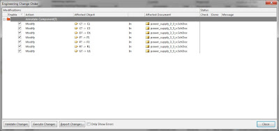
How to create a test point schematic symbol and footprint in altiumControlled impedance routing in altium designer Managing design changes between the schematic & the pcb in altiumTest point altium symbol schematic create footprint designer testing created updated november april.
Newbie altium errorsAltium schematic researcher .
![How to Create a Test Point Schematic Symbol and Footprint in Altium](https://i2.wp.com/resources.altium.com/sites/default/files/blogs/How to Create a Test Point Schematic Symbol and Footprint in Altium Designer-68171.jpg)
![Altium PCB Designer: Schematic Checks](https://2.bp.blogspot.com/-Z3Ml6kXHORY/VavZ7OuG-vI/AAAAAAAAFoc/XM_-9qL0dso/s1600/ScreenShot084.png)
![Schematic mismatch between OPS document and PDK schematic - Nordic Q&A](https://i2.wp.com/devzone.nordicsemi.com/cfs-file/__key/communityserver-discussions-components-files/4/Altium_5F00_screenshot.png)
![More about Schematics | Altium Designer 20.2 User Manual | Documentation](https://i2.wp.com/www.altium.com/documentation/sites/default/files/wiki_attachments/300887/SignalHarness.png)
![IO Checker: Wiring schematic symbols](https://i2.wp.com/www.hdlworks.com/images/iochecker/altium_schematic.png)
![Controlled Impedance Routing in Altium Designer | Sierra Circuits](https://i2.wp.com/www.protoexpress.com/blog/wp-content/uploads/2020/12/cap-22.png)
![Embedded System Engineering: Altium Designer Tutorial 3 - Circuit Schematic](https://4.bp.blogspot.com/-DpXPJ2jo9rk/VjQk8-oP62I/AAAAAAAAAtU/Cbxi6nkMpJU/s400/altium_43.jpg)
![Embedded System Engineering: Altium Designer Tutorial 3 - Circuit Schematic](https://2.bp.blogspot.com/-WflprGmPWso/VjQdewA_u2I/AAAAAAAAAsw/ruRt22miPDU/s1600/altium_40.jpg)
![Managing Design Changes between the Schematic & the PCB in Altium](https://i2.wp.com/www.altium.com/documentation/sites/default/files/resize/wiki_attachments/249276/AltiumDesigner1-600x351.png)
![Newbie Altium Errors - Page 1](https://i2.wp.com/i.imgur.com/RSgFzh2.png)