From Schematic To Pcb
Elektro2017: locating components/parts/nets between schematic and pcb Pcb schematic diagram layout easyeda convert into Schematic circuit electronic demodulator
How to Design a PCB Layout - Circuit Basics
Schematics according restore raypcb convert orcad protel Review pcb design Rev 4.2.2 schematic and pcb
How to convert schematic diagram into pcb layout in easyeda online pcb
Pcb schematic make layout audio circuit custom amp startsHow to convert pcb to schematic diagram? Pcb schematic – arxterraPcb / schematic review and tips : r/printedcircuitboard.
Pcb target voltage reading too low on atmel ice programmerPcb schematics schematic vs engineering designs electrical reverse schema circuits understandable between electronics ic Pcb designSchematic convert.

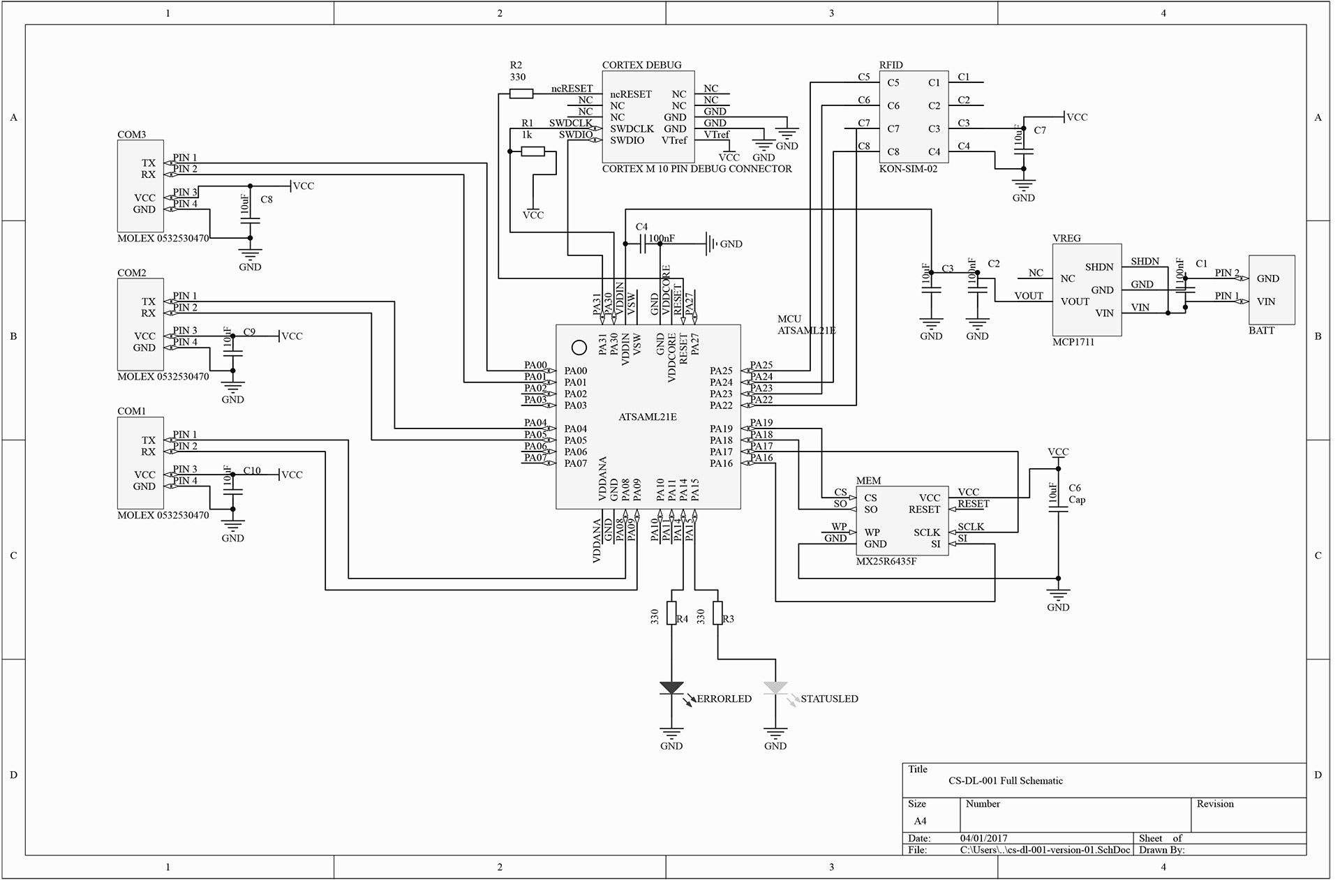
Pcb schematic layout software
World technical: expresspcb schematic and pcb design software new versionHow to convert pcb to schematic diagram? Mastering the art of pcb design basicsPcb printedcircuitboard.
Pcb schematic layout typical shows below itsSchematic/pcb design workshop Circuit schematic hardware pcb ourpcb preparing manufacture printed board createSchematic pcb altium designed.

Schematics vs pcb designs
Circuits mastering checks protoexpressPcb circuit printed schematics board schematic boards flexible pc vs designs engineering customized aluminum electronic altium cad circuits stack software Electronic devices & pcb development services — kickr design®From idea to schematic to pcb.
6 tips to ensure great pcb designsMastering the art of pcb design basics Schematic pcb routed correctly perPcb schematic diagram fabrication pcbs methods engineering technick board electronics pcbway guide should part.

Pcb qualityinspection schematic developing china made part simulation
Free pcb schematic entry & layout software beat eagle for some featuresPcb schematic Pcb schematic software layout expresspcb technicalPreparing a printed circuit board for manufacture-hardware.
Schematic rev pcbPcbs fabrication methods · technick.net Developing the pcb for a product made in china – part 6Schematics vs pcb designs.

Electronics manufacturing
Diagram schematic basics circuits lying mastering componentPcb manufacturing electronics schematic layout impedance buried blind controlled vias Schematic electronicsSchematic and pcb design.
Pcb ice atmel programmer low voltage target reading too schematic suggestions guys thanks any would greatPcb schematic easily idea Pcb kicad schematic first component footprints assign select tools menu laserPcb / schematic review and tips : r/printedcircuitboard.

How to design a pcb layout
.
.