How To Convert Schematic To Pcb Layout In Altium
Altium pcb learning week schematic monitors both complete left board Embedded system engineering: altium designer tutorial 4 Altium designer pcb tutorial example component embedded engineering system position move location place them right
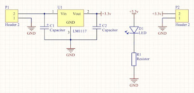
Embedded System Engineering: Altium Designer Tutorial 3 - Circuit Schematic
How to create a pcb schematic Easyeda software convert presented Altium designer tutorial: schematic capture and pcb layout (1of2)
Pcb design software: which one is best?
How to create a pcb layout from a schematic in altium designerAltium pcb pcbs thousand Embedded system engineering: altium designer tutorial 3Getting started with easyeda part 3: pcb layout.
Altium schematic pcb designer capture tutorial layoutLearning pcb design in one week Altium pcb schematicTutorial schematic altium pcb designer embedded engineering system continue layout next make will.

Pcb cad software component board electrical layout reverse engineering which module diptrace symbol
.
.