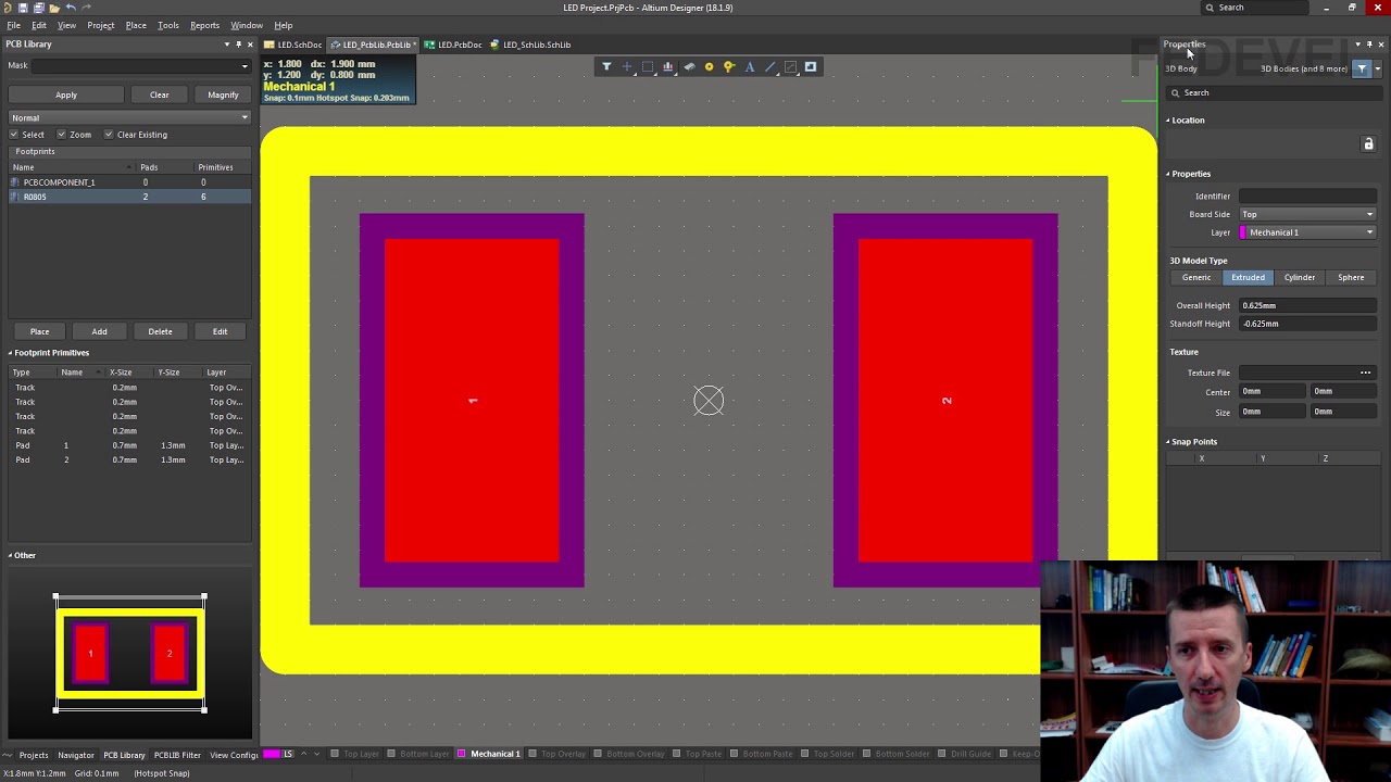
How To Create Footprint In Altium
Altium footprint tutorial Pad altium footprint tutorial Pcb design course
pcb - How to find footprints for Altium - Electrical Engineering Stack
Pcb design course Footprint altium wizard pads length compliant package result fine looks using stack Pcb design course
Altium footprint pcb
Tutorial 2 for altium beginners: how to create footprintsAltium designer tutorial Test point altium symbol schematic create footprint designer testing created updated november aprilAltium footprint tutorial.
Altium find footprints pcbAltium tutorial-6: how to create custom footprint using component Altium schematic documentation footprints designerAltium footprint.
![PCB Design Course - Altium Designer Footprint Creation Tutorial](https://i2.wp.com/911electronic.com/wp-content/uploads/2018/09/43-Via-all.jpg)
Footprint altium create designer wizard ipc ways pcb 3d complian
Schematic placement and editing techniquesHow to create a test point schematic symbol and footprint in altium Pcb design courseHow to create a footprint in altium designer using ipc footprint wizard.
Include ic pin numbers in your altium designer parts dataFootprint : altium Footprint test point altium schematic symbol create designer assignAltium helps finishing include.
![PCB Design Course - Altium Designer Footprint Creation Tutorial](https://i2.wp.com/911electronic.com/wp-content/uploads/2018/09/45-Pad-1.jpg)
How to create a test point schematic symbol and footprint in altium
Footprint altium designerAltium tutorial-5: how to create own footprint-1/how to draw custom Altium menu footprint tutorialPads length in altium footprint wizard.
Altium footprint4 ways to create a footprint in altium designer Altium footprintPcb design course.
![Include IC Pin Numbers in Your Altium Designer Parts Data](https://i2.wp.com/resources.altium.com/sites/default/files/doc_import/iQyM_QdRCIdNTY23k6r5ez24AZJ9BbeaW9gtIYGB-53rfWPwwPZlfEV_mJcvrXS38o2A59Q9x8TIdTXCyScb029hGaVlrhS3GPVHk7Os_ZHYE2c-klzvmcS-5V0YNupC0K6Y2Ayq.png)
![4 Ways to create a footprint in Altium Designer - PCB 3D](https://i2.wp.com/www.pcb-3d.com/wordpress/wp-content/uploads/p/a/create-a-footprint-using-ipc-compliant-footprint-wizard-part-1/021-ipc-compliant-footprint-wizard-next.jpg)
![ALTIUM TUTORIAL-6: How To Create Custom FOOTPRINT Using COMPONENT](https://i.ytimg.com/vi/QeXEUuzHqMY/maxresdefault.jpg)
![Schematic Placement and Editing Techniques | Online Documentation for](https://i2.wp.com/www.altium.com/documentation/sites/default/files/wiki_attachments/248156/FootprintManagerdlgAD15.png)
![Pads length in Altium footprint wizard - Electrical Engineering Stack](https://i2.wp.com/i.stack.imgur.com/BJ5ia.png)
![PCB Design Course - Altium Designer Footprint Creation Tutorial](https://i2.wp.com/911electronic.com/wp-content/uploads/2018/09/11-Ukonczony.jpg)
![Tutorial 2 for Altium Beginners: How to create footprints - YouTube](https://i.ytimg.com/vi/wxYbIGV9_CY/maxresdefault.jpg)
![Footprint : Altium](https://i2.wp.com/external-preview.redd.it/JxIe0v8zE7v5k6tjuXBjLTz6z0C0_7-HkVJ0-TjL2Y4.jpg?auto=webp&s=c7d3370c55e0e87f64a02800a46a8446400f19ff)
![pcb - How to find footprints for Altium - Electrical Engineering Stack](https://i2.wp.com/i.stack.imgur.com/oZZn2.png)
![How to Create a Test Point Schematic Symbol and Footprint in Altium](https://i2.wp.com/resources.altium.com/sites/default/files/inline-images/footprint.png)