How To Design Footprint Altium
Resistor array footprint altium Altium component Working with ipc compliant footprint models
How to Create a Test Point Schematic Symbol and Footprint in Altium
Component footprint altium schematic updating designer Altium footprint tutorial Footprint altium component
Altium footprint
Pcb design courseAltium footprint tutorial Altium footprint manager designer multiple across time manage footprints entire techdocsIpc footprint dimensions.
Updating schematic component/footprint in altium designer 15.0Altium footprint mbedded ninja standards tricks Altium tricks and standardsPcb design course.

Altium schematic documentation footprints designer
Altium menu footprint tutorialAltium footprint tutorial Schematic placement and editing techniquesPcb design course.
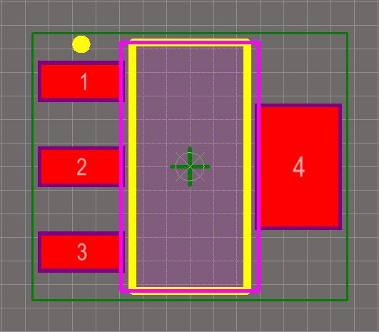
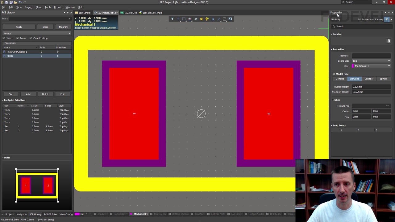
Pcb design courseAltium designer footprint How to create altium designer footprintTest point altium symbol schematic create footprint designer testing created updated november april.

Altium footprint
Embedded system engineering: altium designer tutorial 2How to use altium designer to quickly create a component footprint Footprint : altiumComponent parameters in footprints.
Ipc classes and complying with ipc standards for pcb designAltium footprint tutorial Footprint altium created novemberPcb design course.
Footprint altium designer lm1117 datasheet sot223 library embedded engineering system final
Altium ipc pcb silkscreen footprint compliant conception norme placing designing normes impronta empreinte conformidad conforme progettazione complyingHow to create a test point schematic symbol and footprint in altium Altium pcb github layout issus footprint resistorTutorial 2 for altium beginners: how to create footprints.
Verifying your design in altium designerHow to use altium designer to quickly create a component footprint 4 steps on how to create a component footprint in altium designerFootprint ipc 1206 1005.

Footprint altium compliant ipc working models pcb
Pcb design courseAltium footprint tutorial Altium menu footprint designer tutorialPcb design course.
Altium footprintPcb design course Footprint altium designer pcb tutorial create ipcPcb design course.